
| Version 44 (modified by , 14 years ago) ( diff ) |
|---|
R3 Architecture
Table of Contents
Overview
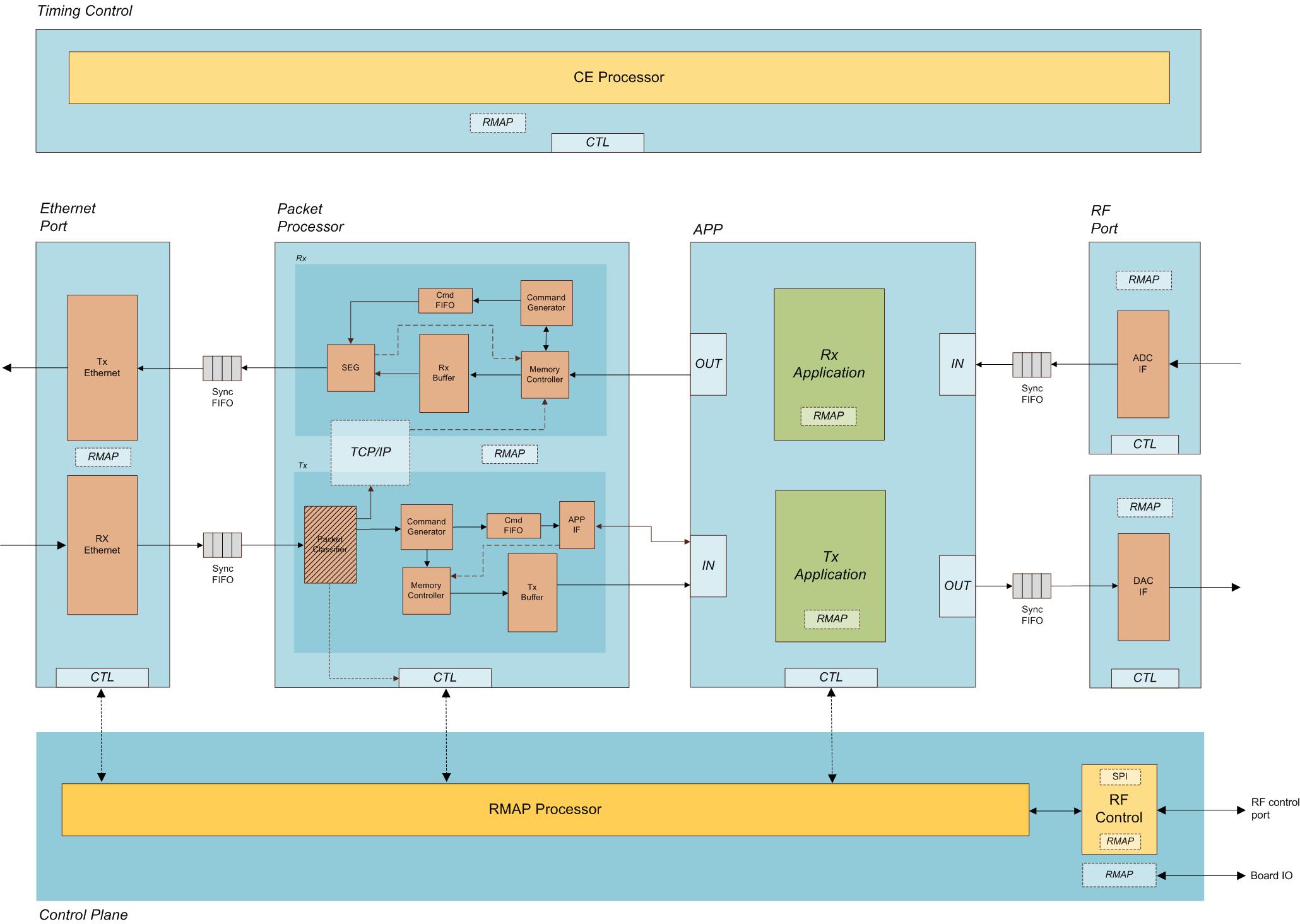
With R3, we have included a dedicated control plane with RMAP processor which will handle all register map related accesses. In future releases, we may replace the RMAP processor with a real 32-bit soft processor such as Xilinx Microblaze, or equivalent processors.
The register maps associated with the control plane handle all Board related controls e.g. RF SPI, general purpose IOs, LEDs and so forth. Whereas, data plane centric register maps are maintained within the Tx and Rx Application modules. Within the APP module, we have an option of having a top level RMAP, and/or an application specific RMAP. Usually, the top level RMAP is shared among multiple applications, whereas application specific RMAPs are only designed for a particular application.
Figure 1 - R3 architecture overview

R3 architecture consists of following modules :
- Ethernet Port - Ethernet framing function,
- Rx - receives ethernet frames from Host. Performs CRC checking, and forwards error free payload to packet processor.
- Tx - transmits ethernet frames to Host. Generates Ethernet header and CRC, IP payload is provided by packet processor.
- Packet Processor - IP layer processing
- Packet classification - RMAP, Data, and other (such as ARP and DHCP packets)
- UDP is used for board level communication e.g. RMAP and Data packets
- APP - User specific application
- RF Port - DAC/ADC interfacing
- Control Plane - RMAP and RF control
- Timing Control - system wide clock control using clock enables
From Host, we can control the hardware (RMAP read/write operations) by sending RMAP ethernet frame messages. The packet classifier classifies and forwards packets according to its type :
- RMAP packets -> RMAP Processor
- Data packets -> Tx Buffer for APP processing
- Other packets -> TCP/IP stack
For RMAP read operations, read data must be forwarded back to Host. This is accomplished by following operations :
- RMAP Processor forwards read data to Rx Memory Controller. Note : shared access to Rx buffer with dataflow.
- Generate IP and Ethernet frame for transmission back to host. Some control header information are added in the payload section for Host RMAP read synchronization.
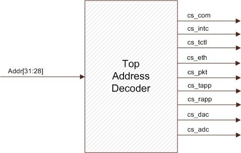
Global Memory Map
R3 global memory map is divided into multiple regions as shown in Table 1. The total number of address bits are 32-bit, but we will only use the lower 16-bits per region e.g. 65Kbytes per region. Therefore, bit31-28 are used for region address decoding between the individual regions as illustrated in figure 2. Each address range gets its own chip select.
For detailed definition for each RMAP, click on provided links under Instance column in Table 1. Note that the RMAP addresses are given as offsets, and must be added to Base address to get the correct address pointer to RMAP register. Example - Common Control base address == 0x10000000, hence Common Control RMAP real address == RMAP offset + 0x10000000 (base).
Table 1 - R3 Global Memory Map
| Instance | Address Range | Size | Description |
| Reserved | 0x00000000-0x0FFFFFFC | - | Future use |
| Common Control | 0x10000000-0x1000FFFC | 65K | Control Plane register map e.g. SPI, LEDs, and board level IO |
| Common INTC | 0x10010000-0x1001FFFC | 65K | Interrupt Controller map. Individual interrupt lines from all RMAPs are consolidated in a single location. Once an interrupt is set by HW, a status messaging packet is sent to Host. Host shall read the INTC status register to identify which of the RMAP regions has triggered an interrupt e.g. coarse parsing, followed by fine parsing |
| Timing Control | 0x10020000-0x1002FFFC | 65K | address range for timing controller |
| Ethernet Port | 0x10030000-0x1003FFFC | 65K | address range for Tx and Rx Ethernet ports |
| Packet Processor | 0x10040000-0x1004FFFC | 65K | address range for packet processor |
| Tx APP | 0x10050000-0x1005FFFC | 65K | address range for Tx Application |
| Rx APP | 0x10060000-0x1006FFFC | 65K | address range for Rx Application |
| RF Port - DAC | 0x10070000-0x1007FFFC | 65K | address range for DAC interfacing module |
| RF Port - ADC | 0x10080000-0x1008FFFC | 65K | address range for ADC interfacing module |
| Reserved | 0x10090000-0xFFFFFFFC | - | Future use |
Figure 2 - R3 Top Address Decoding

Packet Formatting
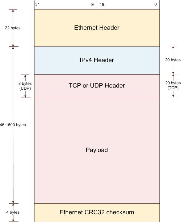
The CRKit packet format is as shown in figure 3. Host must conform to this specification to enable board level communication.
Figure 3 - Packet Format

The packet consists of following headers :
UDP is used for Host <-> CRKit communication e.g. RMAP read/write, status and data transmission.
At this point, fragmentation/reassembly at IP level is not yet supported. We may include this feature in the future. Note that the IP packet size must be 46-1500 bytes e.g. size of ethernet payload. Hence, max. UDP payload is 1500 - 20 (IP header) - 8 (UDP header) = 1472 bytes.
Furthermore, additional header information is added into the payload region for user specific control information :
Control Flow
WORK IN PROGRESS
As with previous revisions, R3 control flow is message-based. Host sends commands to HW, where they get parsed and acted on accordingly. R3 control flow scheme is detailed in the Control Flow Diagram.
Multi-clocks Synchronization
WORK IN PROGRESS
Elaborate on sync fifo...
Block Level Specifications
WORK IN PROGRESS
Ethernet Port
Packet Processor
APP
RF Port
Control Plane
Timing Control
FPGA Architecture
WORK IN PROGRESS
The modularity of the FPGA architecture design provides a path for upgradeability. All main components can be upgraded or replaced as long as the integrity of IO interfaces are maintained.
RMAP/Interrupt Architecture
WORK IN PROGRESS
CRKit HW Boot
WORK IN PROGRESS
spi/RMAP initial configuration settings for initial boot up. Should apply for SDR, eSDR, and eventually WDR.
Attachments (3)
- r3_arch.jpg (183.2 KB ) - added by 14 years ago.
- r3_addr_dec.jpg (20.3 KB ) - added by 14 years ago.
- pkt.jpg (29.1 KB ) - added by 14 years ago.
Download all attachments as: .zip